CXL-GPU: GPU Storage Expansion with World's First Two-Digit Nanosecond Latency CXL Controller IP
Share
This technology brief introduces Panmnesia's GPU storage expansion solution named "CXL-GPU". Check how Panmnesia has constructed a cost-efficient system architecture for large-scale AI, with their world's first two-digit nanosecond latency CXL controller IP.
LARGE-SCALE DEEP LEARNING MODELS: CHALLENGES AND PREVIOUS WORK
Challenges in large-scale deep learning models | Large-scale deep learning models, including large language models and mixtures of experts, have emerged across various computing domains. A primary challenge with these models is that their memory footprints and requirements significantly exceed the available memory capacity of accelerators, particularly GPUs. For instance, while loading and training models with 1 billion parameters necessitate 16~24GB of GPU memory, systems utilizing models with over 100 billion parameters are increasingly common. This surpasses the capacity of current GPUs, which is limited to 80 GB. Consequently, GPUs often have to rely on host memory and storage, requiring frequent data transfers between the CPU and GPU. The requisite data movements not only introduce significant performance overheads but also pose a considerable barrier to GPU adoption. This complexity arises from the need for users to explicitly manage data structures, oversee the transfer of tiled data, and coordinate data migration, processes that can be both cumbersome and inefficient.
Previous work: Unified virtual memory (UVM) | NVIDIA and AMD support their GPU architectures with runtime software for UVM[1]. UVM allows both the CPU and GPU to access data through a shared pointer within a unified virtual address space. Should a memory access request occur for data not currently in the GPU’s memory, this triggers a cache miss and a subsequent page fault. This event prompts a PCIe interrupt, signaling to the host. The host-side runtime software responds by allocating a new page in the GPU memory, transferring the needed data to this page, and updating the GPU. Essentially, memory in the virtual space is allocated on demand. Furthermore, to maintain adherence to a predetermined memory budget, UVM seamlessly replaces older pages in the GPU memory with new data migrations. Thanks to these capabilities, UVM has found widespread use in various frameworks, including TensorFlow[2], DGL[3], and OneAPI[4]. Despite the advantages of UVM in enhancing GPU accessibility, it may induce performance bottlenecks. This performance drop is largely due to the significant latency incurred when the host runtime intervenes to address GPU page faults.
CXL-GPU: GPU STORAGE EXPANSION OVER CXL
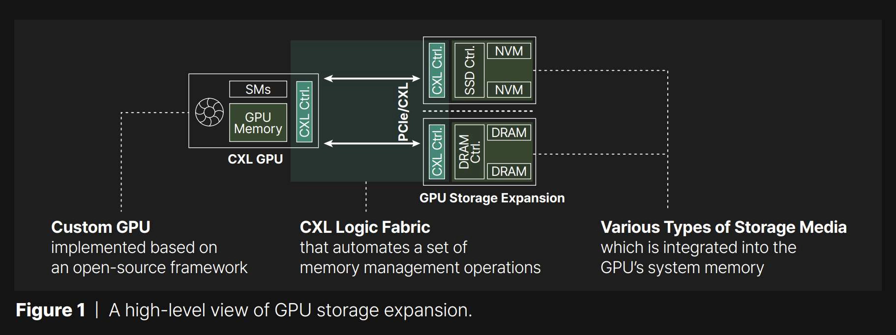
Architecture overview | To overcome the GPU memory capacity limitation with minimized performance drop, Panmnesia introduces GPU storage expansion technology based on compute express link (CXL). Refer to Figure 1 for a high-level overview of the GPU storage expansion approach this paper aims to facilitate. CXL employs the PCIe physical data link to map devices, known as endpoints (EPs), to a cacheable memory space accessible by the host. This setup allows compute units to access EPs directly through standard memory requests. Unlike the synchronous communication of DRAM interfaces defined by JEDEC’s DDR standard, CXL enables asynchronous communication with compute units, similar to block storage. This flexibility permits the implementation of EPs using various storage media, including non-volatile memory (NVM) based SSDs and DRAMs.
World-first two-digit nanosecond latency CXL controller | Nonetheless, integrating CXL for GPU storage expansion poses a notable challenge due to the current lack of a CXL logic fabric and subsystem in GPUs that can support DRAM/SSD EPs as memory expansion devices. In response to the lack of a publicly accessible, comprehensive hardware stack for CXL, we have developed a series of essential hardware layers that support all of the key CXL subprotocols, consolidating these into a unified controller. Figure 2 illustrates the silicon layout of our CXL controller, fabricated using advanced technology from TSMC. This controller is designed for compatibility with CXL 3.1 while also offering backward compatibility with earlier versions of CXL (2.0/1.1). The controller has been rigorously tested, demonstrating a two-digit nanosecond round-trip latency, which includes the time taken for protocol conversion between standard memory operations and CXL flit transmissions. It has been successfully integrated into both a memory expander and GPU/CPU prototypes at the hardware RTL, showcasing its effectiveness and compatibility across a range of computing hardware.
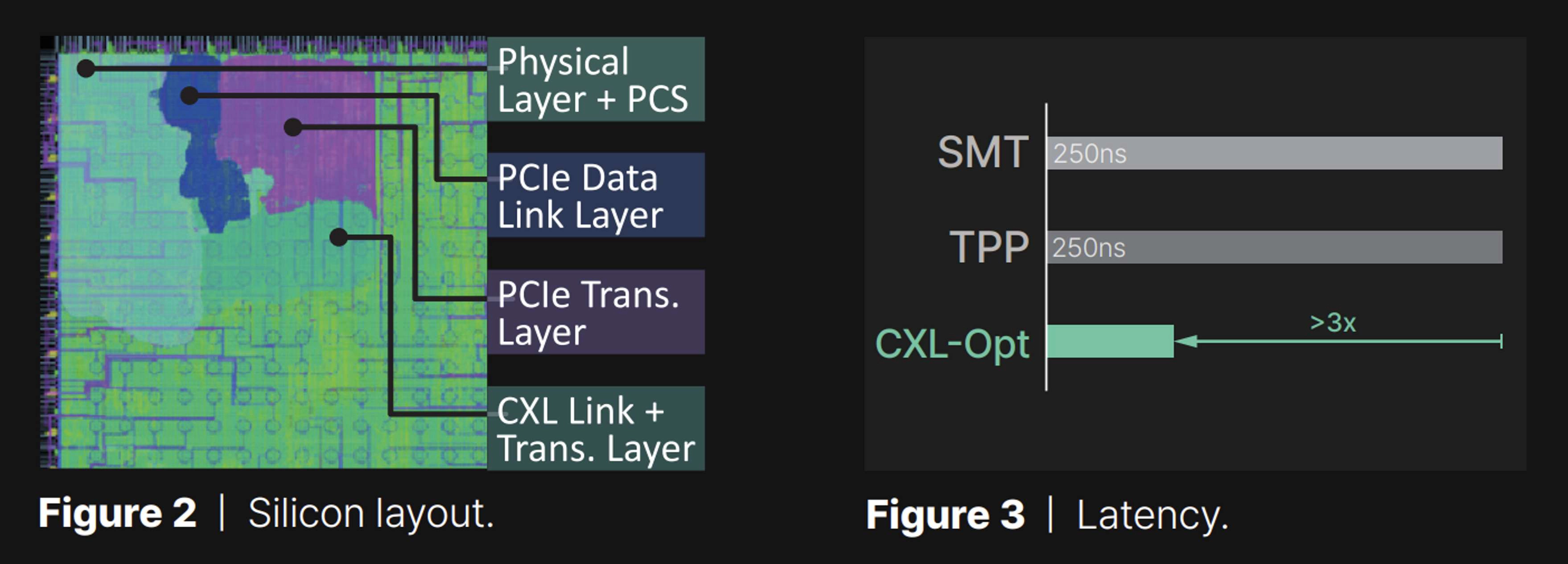
For better understanding, we compare the round-trip latency of our CXL controller (CXL-Opt) with that of SMT[5] and TPP[6]. The results are shown in Figure 3, demonstrating that our controller is more than 3× faster than SMT and TPP. Although there is no publicly available information about their silicon, we conjecture that they leverage PCIe architecture. In contrast, our controller is fully optimized for CXL, from the physical layer to the link layer, and the transaction layer.
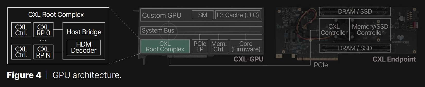
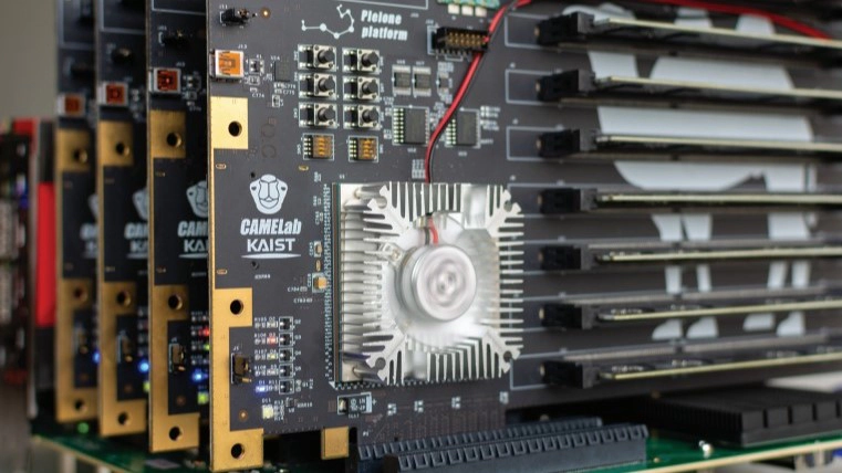
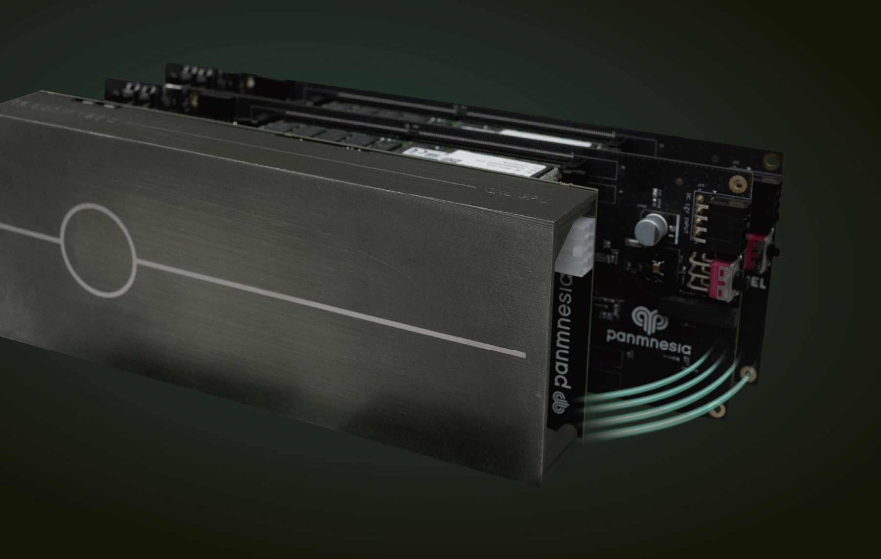
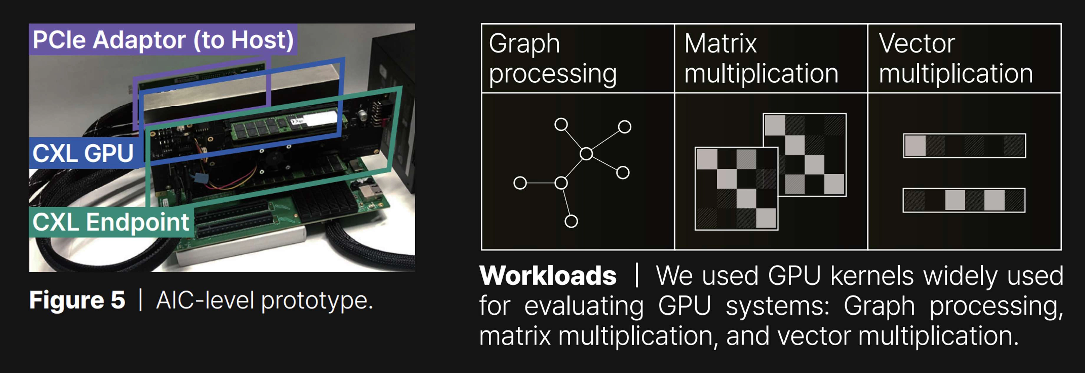
GPU architecture design and integration | In our approach to developing EP devices for GPU storage expansion, we have combined the functionalities of the CXL controller with those of memory/SSD controllers, as shown in Figure 4. This combination enables the CXL controller to extend its backend storage space to the host system, designated as host-managed device memory (HDM). However, integrating with the GPU architecture presents unique challenges due to the requirement for the EP to be recognized by the GPU’s cache system. A straightforward implementation, akin to that used for EPs, is not suitable in this context. To address these challenges, we have developed a specialized CXL root complex (CXL RC) featuring a host bridge equipped with multiple root ports (RP). This configuration is shown on the left side of the figure, where the host bridge connects to a system bus port on one side and several CXL root ports on the other. One of the key components of this setup is an HDM decoder, responsible for managing the address ranges of system memory, referred to as host physical address (HPA), for each root port. These root ports are designed to be flexible and capable of supporting either DRAM or SSD EPs via PCIe connections. Figure 4 also shows the placement of the CXL root complex within the architecture of our custom GPU, which has been developed based on an open-source framework. The systems that integrate our CXL controllers, including the custom GPU and EP, are realized on a 7 nm FPGA-based custom AIC, as depicted in Figure 5.
EVALUATION
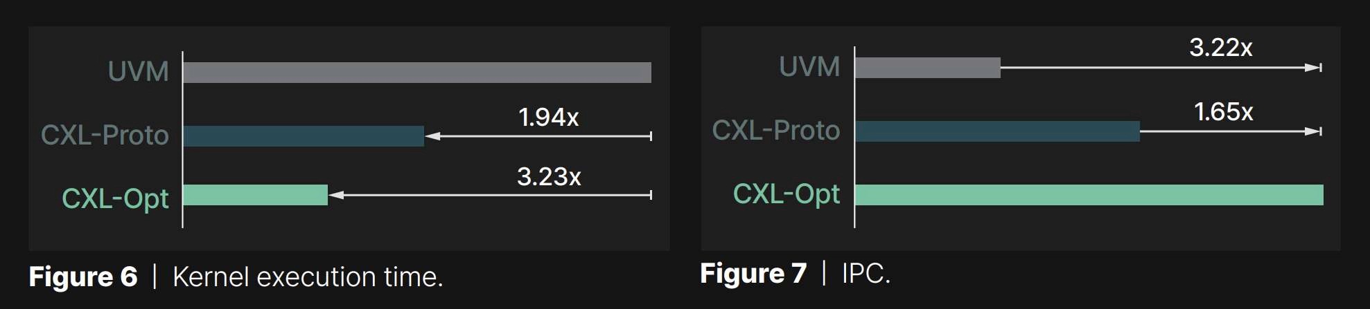
Configurations | We compare three different GPU systems addressing large data challenge. Specifically, UVM1 provides a virtual address space shared across the host and GPU by on-demand memory allocation via page fault. CXL-Proto expands the GPU storage by employing a CXL endpoint prototype that exhibits 250 ns latency, following Samsung[5] and Meta’s report[6]. CXL-Opt also implements GPU storage expansion via CXL, but employs our CXL controller with two-digit nanosecond round-trip latency and additional solutions to optimize the read/write latency.
Performance analysis | Figure 6 compares the execution time of three different systems, and the values are normalized to that of UVM. As shown in the figure, UVM exhibited the worst performance across all GPU kernels we tested. This is because UVM suffers from host runtime intervention overhead when handling GPU page faults. In addition, since UVM migrates the data in the granularity of a page rather than a cacheline, the amount of data transfer is often larger than what the GPU kernel actually needs. In contrast, CXL allows GPU to access the expanded storage via load/store instruction, thereby eliminating the host runtime intervention and unnecessary data transfer issues. This makes CXL-Proto’s execution time 1.94× shorter than UVM. Panmnesia’s CXL-Opt further shortens the execution time by 1.66× by employing an optimized CXL controller exhibiting two-digit nanosecond round-trip latency and additional solutions to hide the read/write latency. This trend can also be observed in Figure 7, which shows the IPC values collected during GPU kernel execution. We can see that Panmnesia’s CXL-Opt shows 3.22x and 1.65x faster performance than UVM and CXL-Proto, respectively.
CONCLUSION
Panmnesia introduces a method to increase GPU storage using CXL technology, integrating DRAM and/or SSDs through CXL multiple root ports. Panmnesia’s custom-designed CXL controller, implemented directly in the hardware, achieves fast response times not seen before in this field. The tests show that this approach improves upon existing solutions, offering a significant step forward in GPU storage capacity and efficiency.
REFERENCES
[1] https://developer.nvidia.com/blog/unified-memory-cuda-beginners/
[2] https://www.tensorflow.org/
[3] https://www.dgl.ai/
[4] https://www.intel.com/content/www/us/en/developer/tools/oneapi/overview.html
[5] K. Kim, H. Kim, J. So, W. Lee, J. Im, S. Park, J. Cho, and H. Song. "SMT: Software defined memory tiering for heterogeneous computing systems with CXL memory expander." IEEE Micro, vol. 43, no. 2, pp. 20–29, 2023.
[6] H. Maruf, H. Wang, A. Dhanotia, J. Weiner, N. Agarwal, P. Bhattacharya, C. Petersen, M. Chowdhury, S. Kanaujia, and P. Chauhan. "TPP: Transparent page placement for CXL-enabled tiered-memory." In Proceedings of the 28th ACM International Conference on Architectural Support for Programming Languages and Operating Systems (ASPLOS), 2023.
Download/Read the Full Technical Report Information about CXL 3.1 Controller IP (Design and Reuse)